- Specialized in SMT requirements
- Measurements directly in the production
- Now with an extensive measuring range from 0.1 to 100 N covering all types of standard, heavy and odd-shapes components.
- Evaluation optimized for finding causes of errors
- Quick and detailed documentation of the results
- Competent and well acquainted consultation with the measuring tasks due to extensive experience from our measurement service.
- Simple answer to the familiar question, "How do you make sure ...?"

CmForce: Force measuring devices for the determination of placement forces on SMT systems from 0.1 to 100 N
CmForce
The CeTaQ CmForce measuring systems are tailored to investigate the dynamic forces occurring during the placement process. We use a placement area instead of the usual single-point sensor which only measures force statically. The difference in these measurement methodologies is a real game changer. This setup allows the placement of real components and simulates a real production process, which when associated with a high sample size, increases the significance of the measured values obtained.
Now with the new released High-Force FMB05, a cutting-edge force measurement device designed to provide unparalleled accuracy in measuring placement forces up to 100 Newtons. This applies to machines equipped with special nozzles and grippers for odd shapes, thick, heavy components or for connectors insertion. This advanced product is the result of extensive research and development, aimed at addressing the needs of Electronic manufacturer industries where precision and reliability are paramount.
With only one measurement, the force and energy output of each individual nozzle is quickly realized. This allows for necessary maintenance, repair or optimization measures to be carried out in a targeted manner. More importantly, it prevents damage to sensitive components during placement. Furthermore, the knowledge gained facilitates the planning of new products, the introduction of new technologies, and helps with investment decisions. Lastly, objective proof of the actual placement forces is increasingly becoming a critical component of audits.
New experiences, findings and requirements from our measurement service form the base for continuous improvement and new future developments. Our wealth of experience from the measurement of thousands of manufacturing lines helps you to efficiently fulfill your measurement tasks and meet demanding quality goals.
On the one hand, the trend is towards ever smaller and thus more sensitive SMD components. To avoid damage during placement, the transmitted energy pulses (mass multiplied by speed) must be minimized. For a given mass of the component and the moving parts of the placement tool, the speed at which the component hits the placement surface must therefore be low.
At the same time there is a demand for even shorter processing times. This inevitably involves high speeds of movement of the placement tools. For the reliable damage-free placement of chip components in particular, it must be ensured that these impact speeds are not transferred into the component in the form of an energy pulse.
However, it is difficult to make an assessment with the methods of quality assurance commonly used today. As a rule, components are not completely destroyed during placement, but only pre-damaged in a state called a microfracture.

The picture above is from the TEFLON research project between IAVT of TU Dresden and CeTaQ GmbH. It shows an overloaded 0402 chip resistor. Clearly visible are the broken component body and the deformed solder deposits. The resistor layer is still intact. This means that the component will most likely pass all subsequent quality controls such as optical inspection, in-circuit or functional test. Due to the broken body, however, there is a risk of provoking an early failure in the field.
The results can be used, for example, to make statements about the energies applied to a component.

The above example contains the force-time diagram of two assemblies. The first shows a clear impact. The reason comes from a high impact speed of the component and placement tool on the PCB and causes high energy transmission into the component. A curve of this kind can potentially damage a component.
In addition to the force-time curve of individual placement sequences, the function and maintenance condition of a placement head can be assessed. For example, dirty guides lead to an increased scattering of the individual nozzles. If known, the maintenance intervals can be adjusted accordingly.

Mechanical defects of individual nozzles can also be specifically detected and repaired.


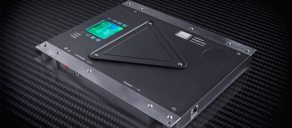
Force Measurement Board (FMB)
The central component of the measuring system is a sensor board with a triangular measuring surface of about 5000 mm². This allows a sequence similar to the assembly of real printed circuit boards. The necessary measuring electronics are integrated in the board. Forces acting on the sensor surface are recorded and analyzed by the CmForce software.
The sensor board can be fed into the placement machine like a normal PCB and processed similar to production PCBs. The measuring surface offers sufficient space for the assembly with real components in statistically relevant volumes. This means that all dynamic influences occurring during regular production are included in the measured result.
The sensor board enables the measurement of all common placement machines, utilizing any component size, and functions completely independent of the manufacturer.
CmForce Software
The corresponding software CmForce analyses and saves the measurement results. The most important features are:
- Live display of the force-time curve during placing
- Detailed analysis of the force-time curves
- Immediate results for quick decisions
- Various peak search algorithms
- Maximum peak forces of the assembly sequence
- Pulse force (dF/dt) - energy input into the component
- Duration of placement
- Head/nozzle evaluation
- Statistical evaluations
- One click HTML protocol with all results
- Calculation of capability characteristics
- Data export for CmCStat6.0 Expert
Procedure of a Measurement
Before the first measurement, a corresponding placement program must be available or created. We recommend setting at least 25 components per placement tool. If the program is available on the pick and place machine, the sensor board will be processed like a real PCB. Generally, components from production are used for this purpose. As well, we recommend using the smallest, most challenging, relevant or interesting component types.
The required measuring time is essentially the same as the placement time, i. e. relatively short. After the measurement, the data is analyzed. The software allows to break down the measured values down to the individual nozzles. If the results show problems such as worn or stiff springs, they can be specifically corrected in a targeted manner.
At the end, a report can be generated with one click to document the condition of the equipment.
Customers who own a CmController with CmCStat6.0 Expert also have the possibility to export the data and analyze, document and archive them in CmCStat6.0.
There are three different systems to choose from. The FMB-03 is a wired system, 175 mm large with a measuring range between 0.1-20N. The FMB-05 is a wireless system, 210 mm large with two different measuring range (Stamdard and High-Force). The previous FMB-04 is no longer sold.
Technical Specifications
- Dimensions: 232 x 175 x 15 mm
- Board edge thickness: 1.5 mm
- Weight: approx. 1 kg
- Measuring range: 0.1 – 20.0 N (full area)
- Measurement uncertainty (U): \(\pm 0.03\) N
- Assembly space: approx. 5000 mm²
- Measurement frequency: 10 – 50,000 Hz
- Data transmission: USB cable
- Dimensions: 257 x 210 x 25 mm
- Board edge thickness: 1.5 mm
- Weight: approx. 2 kg
- Measuring range:
- Standard: 0.1 – 20 N
- High-Force: 0.1 – 100 N
- Measurement uncertainty (U):
- Standard: \(\pm 0.03\) N
- High-Force: \(\pm 0.02\) N + \(\pm 0.01\) N x Nominal [N]
- Assembly space: approx. 5000 mm²
- Measurement frequency: 10 – 50,000 Hz
- Data transmission: WIFI