- 3D glass roughened and coated
- Standard heights of 3D structures: 50 µm und 100 µm
- Size 3D-Board: 175 mm x 175 mm
- Glass substrate size: ca. 125 mm x 125 mm
- Optional Calibration certificate for x/y accuracy and height (Standard or Standard Plus)

3D Glass Measuring Plate for SPI Verification
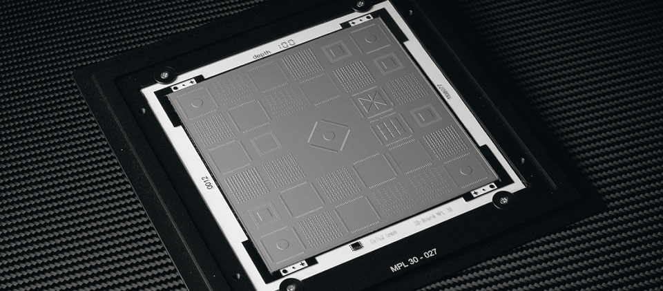
3D-SPI Board
Efficient and cost-effective surface mounting (SMT) requires a high degree of process know-how. The first process step, solder paste printing, is generally considered crucial for product quality. On the one hand, a precise paste application lays the foundation stone for the soldering joint. On the other hand, any errors that have been found can be corrected relatively inexpensively. Accordingly, automatic inspection systems for paste application (SPI Solder Paste Inspection) are very popular. These systems provide measurement values of relevant process parameters of the soldering paste printing. In general, these are: x-, y-positions, height, volume and area of the transferred depots. The information can be used on the one hand for direct process control and on the other hand also for evaluating the processability of the products. The knowledge of this enables a targeted work on fault centres and thus an improvement of the production quality. The reliable extraction of process-relevant data is also interesting under the slogan "Industry 4.0"
An example of the use of the measured values for direct process control is the observation of the transferred solder volume and the depot height over time. If an increase becomes noticeable here, this indicates a contamination of the lower surface of the stencil. If one recognises such a phenomenon, one can counteract it with an underside cleaning. Against this background, the automatic feedback of measurement results from the SPI into the printer seems to be an effective means of improving production quality. Many SPI-manufacturers nowadays offer corresponding interfaces for the correction of printing misalignment. In addition, there are efforts to intervene in the assembly process by means of the measured pad positions - i. e., the position of the components should be adapted to the measured pad positions. At this point at the latest, the automatic inspection system becomes an automatic measuring system and the question of measuring accuracy must be asked.
Technical Specifications
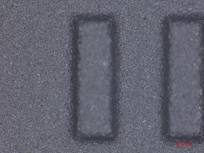
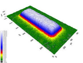
With the reference normals available on the market up to now, a corresponding verification was only insufficiently possible, since no structures common in the SMT process were available on the boards. CeTaQ has taken up this challenge and developed a reference board to investigate the measurement capability of SPI systems. The core is a three-dimensional structured glass substrate. It is embedded in an aluminium carrier that protects the substrate and allows easy handling in an SMT production line. The surface of the glass substrate is roughened and coated with a chromium layer. By default, it is silver-grey and reflects the entire light spectrum. The structures in the glass are typical of printed circuit boards in SMT production, and manufacturing defects such as solder bridges on the board have also been reproduced. For most SPI systems the structures look like normal solder paste depots. Here is a picture of a QFP pin taken by an SPI machine and a model created by a measuring device with a laser scanner.
Measurement procedure
For the examination of the measuring accuracy, the reference board is passed through the system and measured several times. The recorded data is exported and evaluated with our statistics software CmCStat. The SPI user creates the necessary program with the help of a Gerber file. The reference to the pads on the board is made via a corresponding PIN-CAD file. Typically, the evaluation is carried out with different orientations of the board in the system. This means that the board is first measured with 0 degrees and then with 180 degrees of orientation. The reproducibility of the same pads is evaluated. With this procedure, any potential rotation errors are included in the valuation.

Furthermore, the influences of different pad geometries are made visible.
Often the measured actual value is directly related to the pad size.
Smaller pads are usually measured too flat.

Technical data
- Fiducials for Global Position Recognition
- two-poles: 0201, 0402, 0603
- QFP: TQFP80, TQFP100, TQFP128
- BGA: BGA228
- ground planes
- Defect structures: solder bridges, solder beads, defects and incomplete pads
- Positional accuracy of the 3D structures < +/- 5 µm
- Positional accuracy of the fiducial < +/- 3 µm
- Constant height over the entire board < +/- 2% (The height of the structure to the surrounding area)